The field of printed circuit board (PCB) finishing and bonding methods has been growing and diversifying for decades. PCB design depends heavily on the use and environment of the electronic package, and those design decisions include what Surface Mount Technology (SMT) is employed. SMT involves the finish, the bonding and soldering method, flux cleaning, reflow and curing, wire bonding, and any other operations that are used to apply components to the surface of circuit boards.
For high-reliability applications, such as electronics used in military and defense aerospace, Electroless Nickel Immersion Gold or ENIG is the most common finish utilized. The strength of this finish makes it ideal for preserving the life and performance of hi-rel electronics in systems like long range Surface-to-air missile systems and systems used to track projectiles, communicate, and navigate.
In this article, we’ll explore some of the problems that can occur with ENIG and how to make sure they don’t appear in your PCB assembly process.
Building PCBs for Electrical Performance
Most PCBs are designed with copper finishes on a raw, unpopulated surface. Copper is a highly reactive metal, and if left exposed, the copper surface will oxidize and quickly deteriorate, ruining the circuit board. The surface finish exists to create a protective barrier over the copper circuitry and to provide a solderable surface when assembling the components onto the board.
Choosing the appropriate surface finish and ensuring that the finish itself is clean and fully prepared to be bonded or soldered gives you a critical interface between the component and the PCB. Finishes are chosen with the end product in mind, and some of the considerations in choosing the best finish include:
- Versatility
- Cost of metals or other materials
- Life span
- Re-usability
- Harmful materials involved (carcinogens, lead content, etc.)
- How flat the finish is
- Difficulty of application
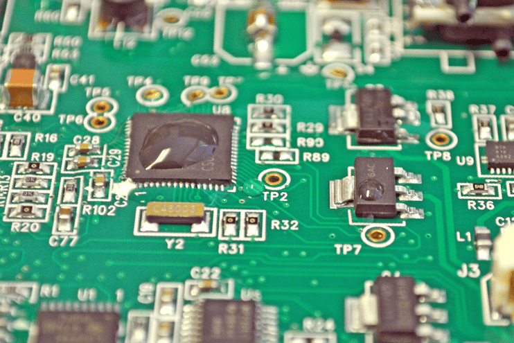
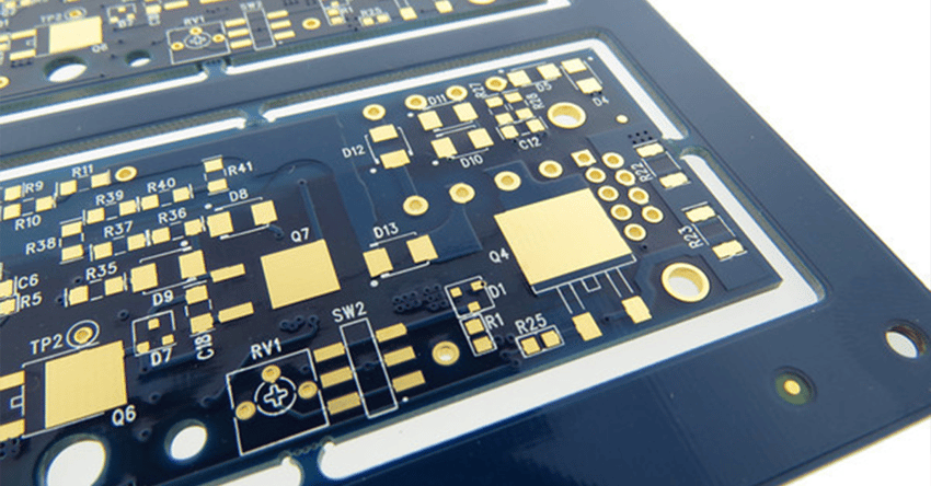
ENIG is a flat, lead-free finish that has great durability and, as such, has become one of the most widely utilized PCB surface finishes. In order to mount components onto an ENIG surface, you have to make absolutely sure that it is truly ready to be soldered to, bonded, or coated.
What is ENIG (Electroless Nickle Immersion Gold) in Surface Finishes?
ENIG, or Electroless Nickel Immersion Gold, is a two-layer ENIG plating process where a thin layer of electroless nickel is applied to a printed circuit board surface (the layer of nickel is about 120-240 μin thick), followed by a thin layer of immersion gold plating (the gold thickness is about 2-8 μin thick). The nickel protects the copper on the board, and the purpose of the gold plating is to extend the shelf-life of the package by ensuring the nickel is corrosion-resistant during storage and before the assembly of the board.
Other common types of surface finishes are:
- HASL (Hot Air Solder Leveling)
- Immersion Tin
- Immersion Silver
- OSP (Organic Solderability Preservative)
- Hard Gold
All of these solve the basic problem of copper wiring vulnerability to ensure high-performance conductivity. The surface finishes of each require proper handling, surface treatment, and cleanliness verification to ensure the successful bonding of the components. ENIG, however, has been established as the preferable solder mount method for high-reliability electronics applications with complex circuitry design.
Download our checklist to diagnose the root cause of adhesion failures you’re experiencing in your PCB manufacturing process: Checklist: Adhesion Failure Root-Cause Analysis for Manufacturers
Problems with ENIG Surface Finishing
Manufacturers of PCBs generally take great care when handling boards and components to ensure no damage comes to them. Wearing gloves and using fully sealed packaging go a long way to preserve the shelf life and usability of electronic components. Protecting them from corrosion due to moisture, finger oils, and other environmental contaminants is extremely important. All of these are possible root causes of contamination and problems down the line.
ENIG is also susceptible to a particular kind of corrosion called “black pad,” where the nickel has broken down more than desired (some nickel oxidation is required for the gold plating to form a coating on the nickel) and increases the amount of phosphorus. When the nickel is corroded due to over-oxidation or dissolving during the solder reflow (oven curing) phase, the nickel appears darker and becomes brittle.
However, there are a few areas of the circuit board assembly process that typically go uncontrolled and could allow adhesion failures like dewetting, non-uniform coatings, corrosion, dendrite growth, shorts in the board, and many other unpleasant issues.
Ways to Control ENIG Surface Finishes
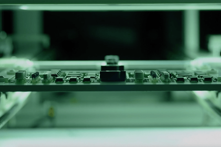
Once PCBs have had the ENIG finish applied, they often go into storage in batches and await their chance to be populated with small components. These components will be soldered, adhered, wire-bonded, sintered, and attached in other ways to the surface mount pads on the ENIG finished boards.
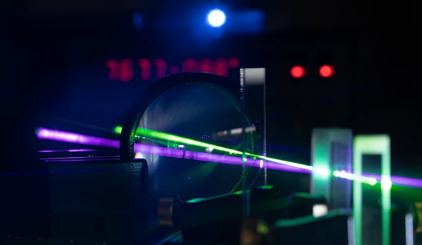
Plasma treatment or plasma cleaning is a way to activate a surface by engineering a chemically compatible assortment of molecules at the first few molecular layers of the materials being bonded.
Let’s put it another way. When the ENIG substrate is sitting in storage (or anytime after it’s been applied to the PCB), the chemical characteristics of the very top few layers of molecules of its surface may not be particularly interested in adhering to the very top few layers of molecules of the silver, epoxy, wires or other materials that it is going to try to bond with once the assembling gets underway. So, the molecules on those top few layers need to be changed or removed so molecules that are interested in bonding can make their home on the surface.
The role of plasma treatment in this is to bombard the surface of that ENIG with a gas that alters the chemical makeup of the surface. Adhesion of any kind is a chemical phenomenon that requires a certain set of amenable molecules to exist on both surfaces that are joining together to form the interfacial bond. Vacuum plasma is a common treatment method because it is able to get into extremely tiny spaces for precision chemical cleaning. Chemical cleaning is what we call getting the chemical recipe of the surface just right.
Vacuum plasma treatment works by introducing an ionized gas to a chamber where a vacuum has been pulled. The PCB is placed in the chamber, and the gas interacts with the surface to clean it of organic impurities and alter its chemistry.
It is extremely important to bear in mind that the kind of cleaning plasma does is not the kind of cleaning an ultrasonic bath does. If there is a substance, such as an oil or silicone, on the surface, the plasma will be interacting with that substance and not the surface of the substrate that the operators are hoping to clean. With enough power and time, plasma can remove certain substances from a surface, but it is always crucial to understand where that power should be concentrated. When you over-treat a surface, you can volatilize the surface and cause damage that is not possible to recover from.
In order to use plasma most effectively, you need to know exactly what your surface looks like going into the treatment and what it looks like coming out.
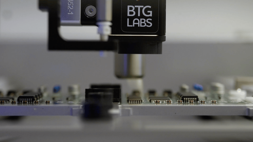
Understanding how plasma treatment works and its effect on adhesion during the ENIG process is the first step to controlling the outcomes. But to accomplish that more precisely, you need to be able to measure the surface cleanliness of your board before and after treatment. Getting a baseline of surface quality before the boards go into the chamber and then getting a quantitative reading on the cleanliness once the boards have gone through the treatment gives you a thorough picture of how much the surface is changing.
Using surface quality measurement equipment as a process control method lets you know how efficacious your treatment process is. Like all quality control methodologies, developing specifications, metrics, and standards create predictable outcomes, lower scrap rates, and higher-quality products. Putting a specification on surface quality before and after treatment gives you the opportunity to optimize your surface preparation equipment.
Dialing in the proper cycle time and power of the plasma unit allows the treatment process to do its job - removing contamination and creating a bond-ready surface. It is also important to measure the cleanliness within the vacuum chamber to ensure there are no unintended contaminants being deposited on the surface of materials being placed inside the chamber. Chamber cleanliness is an often overlooked Critical Control Point in the adhesion process of PCB manufacturing.
Other Non-Obvious Variables That Could Be the Root Cause of Adhesion Issues
When the components have been applied to the epoxy on the ENIG during the assembling of a populated circuit board, the whole package will be cured in an autoclave or oven. To ensure even curing and heat transfer, oftentimes, a silicon rubber press pad will be laid on top of the components. This applies the right amount of pressure and is an extremely gentle process, but as the curing happens, the silicone can become mobile, contaminating the board.
Silicone can be one of the most detrimental contaminants to adhesion. Many suppliers of these pads have designed them to be resilient to these high temperatures, but in order to be absolutely certain you’re not inadvertently introducing unwanted substances (contaminants) to your PCB, it is imperative that you have a way of measuring the chemical cleanliness of your board before and after curing.
We’ve talked a lot about the board, but one of the least controlled areas of cleanliness in electronics manufacturing is the surface quality of the components that populate the boards. These chips need to be chemically compatible with the adhesion requirements in the same way that the ENIG is. Not only do the surfaces need to be clean to bond with the board, but the side that will eventually have a conformal Parylene coating applied to it needs to be clean as well.
Manufacturers expect that the components they are receiving from suppliers are clean and ready for assembly. But without a surface quality specification on all incoming parts and supplies, it’s a guess what contamination might be making its way into the process by way of the supply chain.
One of the most pivotal Critical Control Points is before any handling or treatment is even done by the manufacturer. Measuring surface quality at the outset and requiring suppliers to provide assurances of the cleanliness of the parts they provide go a very long way to building predictability into every downstream operation.
A Measured Process is an Effective Process
Manufacturing electronics involves a lot of bonding and coating. Every interfacial bond is vulnerable to contamination, and therefore, the chemical cleanliness of every surface needs to be measured and understood throughout the entire adhesion process. This process begins before the cleaning and after the assembly. Every aspect is connected, and in order to create a process that allows for high reliability, you need to measure the surface quality and control the outcomes.
To learn more about diagnosing the root cause of adhesion failures in PCB manufacturing and how to control the outcomes of bonding to ENIG, download our eBook: Electronics Manufacturing: The Complete Guide to Implementing a New Approach to Increase Quality.

Thank you to EPEC: Engineered Technologies for use of their Images, all image rights reserved to EPEC.